SV-LLM: An Agentic Approach for SoC Security Verification using Large Language Models
DeepC: Agentic RAG for Intelligent and Secure RTL IP Reuse
FAME: Fault-Injection Assessment and Mitigation of Microelectronics at Pre-silicon
SVH: Security Verification of Heterogenous Integration
Automated Rule Checking for Hardware Security
CAD Framework for Detecting and Mitigating Security Vulnerabilities in High-level Synthesis
Automated Verification and Debugging using Formal Methods
Design Automation of Modeling IoT Devices
Verification of IoT System-on-Chips
Post-Silicon Validation and Debug
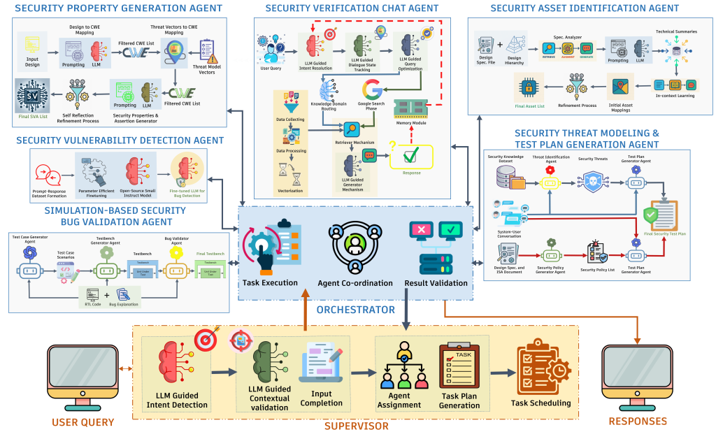
SV-LLM: An Agentic Approach for SoC Security Verification using Large Language Models
Ensuring the security of complex system-on-chips (SoCs) designs is a critical imperative, yet traditional verification techniques struggle to keep pace due to significant challenges in automation, scalability, comprehensiveness, and adaptability. The advent of large language models (LLMs), with their remarkable capabilities in natural language understanding, code generation, and advanced reasoning, presents a new paradigm for tackling these issues. Moving beyond monolithic models, an agentic approach allows for the creation of multi-agent systems where specialized LLMs collaborate to solve complex problems more effectively. Recognizing this opportunity, we introduce SV-LLM, a novel multi-agent assistant system designed to automate and enhance SoC security verification. By integrating specialized agents for tasks like verification question answering, security asset identification, threat modeling, test plan and property generation, vulnerability detection, and simulation-based bug validation, SV-LLM streamlines the workflow. To optimize their performance in these diverse tasks, agents leverage different learning paradigms, such as in-context learning, fine-tuning, and retrieval-augmented generation (RAG). The system aims to reduce manual intervention, improve accuracy, and accelerate security analysis, supporting proactive identification and mitigation of risks early in the design cycle. We demonstrate its potential to transform hardware security practices through illustrative case studies and experiments that showcase its applicability and efficacy.
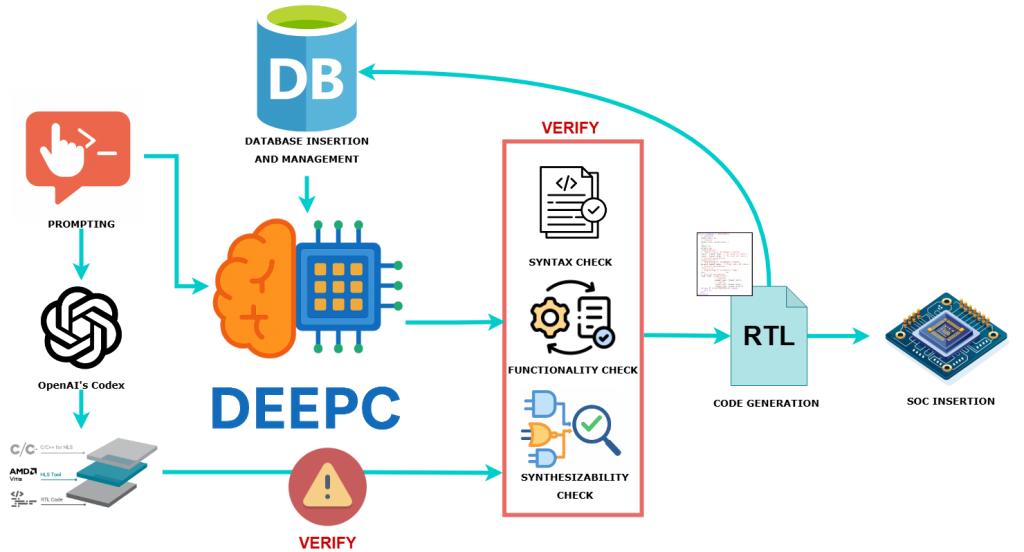
DeepC: Agentic RAG for Intelligent and Secure RTL IP Reuse
With the emergence of large language models (LLMs) in design automation, many academic efforts have focused on improving register-transfer level (RTL) code generation. However, industry design teams face a more pressing challenge: the need to rapidly adapt and reuse existing IP blocks for evolving specifications, specifically with security and correctness at the forefront. DeepC is a novel agentic retrieval-augmented generation (RAG) solution designed to meet this demand. It enables intelligent, LLM-driven IP modification for reuse, reducing the friction in adapting legacy or third-party designs to meet new design and verification requirements. DeepC is built on VerilogDB, the largest and highest-quality open-source Verilog dataset available, and pairs it with advanced prompt engineering and a rapid, agentic generation loop. By combining intelligent retrieval with generative adaptation, DeepC enables faster, more secure, and more scalable IP reuse, bringing LLMs one step closer to practical deployment in real-world chip design and hardware verification pipelines.With the emergence of large language models (LLMs) in design automation, many academic efforts have focused on improving register-transfer level (RTL) code generation. However, industry design teams face a more pressing challenge: the need to rapidly adapt and reuse existing IP blocks for evolving specifications, specifically with security and correctness at the forefront. DeepC is a novel agentic retrieval-augmented generation (RAG) solution designed to meet this demand. It enables intelligent, LLM-driven IP modification for reuse, reducing the friction in adapting legacy or third-party designs to meet new design and verification requirements. DeepC is built on VerilogDB, the largest and highest-quality open-source Verilog dataset available, and pairs it with advanced prompt engineering and a rapid, agentic generation loop. By combining intelligent retrieval with generative adaptation, DeepC enables faster, more secure, and more scalable IP reuse, bringing LLMs one step closer to practical deployment in real-world chip design and hardware verification pipelines.
FAME: Fault-Injection Assessment and Mitigation of Microelectronics at Pre-silicon
With the emergence of the Internet of Things (IoT) and edge computing that promises new and exciting applications from the military, naval, mobile, financial, transportation, and household sectors, security and privacy have emerged as major design challenges. The computing and sensing components in an IoT system, cryptographic hardware in embedded systems, reconfigurable Field Programmable Gate Arrays (FPGA) embedded systems, artificial intelligence (AI) accelerators, digital signal processors (DSPs), and microprocessors are all highly vulnerable to diverse forms of physical and non-physical attacks. These attacks appear in different forms (e.g., information leakage, side-channel leakage, fault injection, physical attacks, rowhammer) and can effectively bypass the security mechanisms built in a design, thus putting systems at risk. Among them, fault-injection attacks have become a major concern to the computer security community primarily due to their powerful capability in tampering with critical features in a device and ability to extract secrets, irrespective of the mathematical strength and robustness of the implemented security mechanisms.
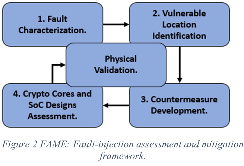
Researchers have proposed physical or design techniques [15-21] to counter fault-injection attacks. However, most of the countermeasures are expensive with large overhead and design effort, making them limited to deploy in practice. Therefore, one possible approach is to find the most vulnerable locations in a design to fault attack and place emphasis on protecting these vulnerable locations so that the countermeasure would be more efficient, and the overhead would be greatly reduced.
Sponsors: ONR, Ansys
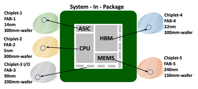
SVH: Security Verification of Heterogenous Integration
HI (as shown in the illustration) allows separately fabricated components such as chiplets (custom-made silicon die for a specific application) to work together to form a higher-level assembly, the SiP.
The move towards HI is primarily driven by three factors. First, technological diversity – various chiplets with different technology nodes and foundries can be integrated on the same package using an intermediate silicon layer called interposer. Second, functional diversity – individual components such as chiplets (memory, logic, or I/O) or MEMS sensors can be integrated into a single package. Third, materials diversity – newer materials can be used to optimize the chiplet for a specific function and capabilities.
SECURITY VERIFICATION
With the increased complexities of SiPs, conventional pre- and post-silicon verification techniques can’t be applied to fabricated chiplets, making SiP security verification quite challenging and unique. To address these concerns, the work outlined in the NSF project will pursue two parallel approaches: static security verification and runtime security property monitoring.
Static Security Verification
Utilizing the system specification (usually provided by the customer or design house), the team will develop security policies/properties to ensure confidentiality, integrity, and availability requirements for targeting security-critical assets and to provide mitigation strategies if any of the policies are violated.
Runtime Security Property Monitoring
A promising solution would be to add at-speed security monitoring capabilities to the package itself, thereby enabling runtime security policy/property checking and enforcement. Runtime security policy can be done using an innovative integrated chiplet hardware security module (CHSM), implemented using an embedded FPGA fabric. Using existing tools, these CHSMs are embedded as additional modules in chiplets. The CHSM can subsequently be updated to respond to unknown and zero-day attacks. This innovative approach is believed to be the first-ever comprehensive security verification technique specifically for SiPs. The hope is that this new method will prove to be capable of identifying and mitigating vulnerabilities during pre- and post-silicon, as well as at runtime.
Sponsors: ONR, Ansys
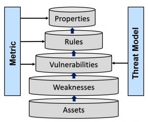
Automated Rule Checking for Hardware Security
Security properties are the rules, usually represented in a formal language, which are expected to be maintained by a particular design. During the security property-based verification, a set of security properties is developed for a specific threat model and verified using model-checking tools to ensure the design does not have any vulnerabilities leading to the corresponding threat.
System-on-chips (SoCs) are increasingly being used in high assurance electronic systems such as military, space, automotive, banks, health care, etc. These systems have strict security requirements because their failure can damage major financial infrastructure, endanger personal privacy, and undermine the viability of whole business sector. It has been demonstrated that the security of SoCs can be compromised using information leakage, timing and power side-channel attacks, exploitation of design-for-test (DFT) structures, and fault-injection attacks. These attacks can effectively bypass the security mechanisms built in the software level and put chips or systems at risk. Further, due to the globalization of the semiconductor design and fabrication process, SoCs are vulnerable to malicious modifications, referred to as hardware Trojans, during design process (from RTL to Gate level to Physical Design) and manufacturing phase. Apart from the vulnerabilities exposed by these attacks, many security vulnerabilities in SoCs can be unintentionally created by design mistakes and the designer’s lack of understanding of security problems. Further, computer-aided design (CAD) tools can introduce additional vulnerabilities in the SoC unintentionally. The objective of this projectl is to develop a comprehensive framework for automated rule checking for hardware security, for analyzing the security issues and vulnerabilities in SoC designs, including potential untrusted third-party IPs, from RTL to layout.
In this project, we aim to
- Develop novel and efficient security properties and security-aware design rules to systematically identify security issues and vulnerabilities during pre-silicon design and verification stage
- Assess how critical the vulnerability is with design-level metrics, rules, and threat levels
- Allow design-level fixes, with automation and integrated tool sets for asset protection and address security vulnerabilities as early as possible in the design process
- Provide guidance to the designers for risk versus effort assessment based on the security level
In the SRC project, a novel security property mapping mechanism is proposed which can translate the properties from one abstraction level to another and between different versions of the designs. At the same time, we identify new vulnerabilities introduced while the design moves from the higher to the lower abstraction levels in the design flow. In this project, we propose a framework, called Automap, that aims reducing security verification efforts by mapping the security properties at different design stages (e.g., C/C++/systemC, RTL, Gate-level) and design versions to lower the total verification time.
Sponsors: DARPA, SRC
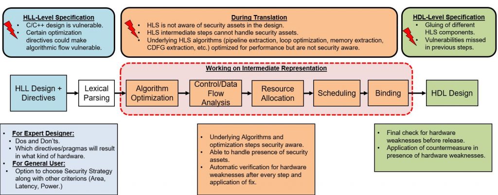
CAD Framework for Detecting and Mitigating Security Vulnerabilities in High-level Synthesis
High-level Synthesis (HLS) is an effective solution to cope with the ever-growing demand for increasing design and verification productivity of semiconductor design flow, especially with the emergence of artificial intelligence (AI) hardware and FPGA-as-a-service. It offers unparalleled possibility of speeding up the time-to-market by allowing the design and verification engineers to implement efficiently complex algorithms as well as custom logics design in higher levels of abstraction, e.g., C/C++. HLS is increasingly being adopted by government (e.g., DARPA CRAFT program) and commercial (e.g., Nvidia, Qualcomm, Intel, and Mentor Graphics) entities. Although, many research endeavors have been directed to optimize and increase the efficiency of HLS (e.g., GRC Task 2807.001, 2506.001), none have investigated potential security vulnerabilities introduced by HLS and to identify and mitigate these vulnerabilities automatically. Security vulnerabilities introduced by HLS during transformation could be exploited to leak sensitive information and perform other possible attacks e.g., denial of service, reduction in reliability, etc.
In this project, we plan to (1) investigate potential security issues introduced by the high-level synthesis (HLS) process, (2) develop CAD framework to identify these security vulnerabilities in an automated manner, and (3) develop secure high-level coding practices and countermeasures (similar to Cert-C) to help prevent such vulnerabilities during HLS.
Project Budget: $23,515
Current Sponsors: SRC, DARPA
Automated Verification and Debugging using Formal Methods
In our past projects, we proposed a novel verification technique using Gröbner basis theory to formulate the equivalence checking problem as an ideal membership testing in the algebraic domain and achieve an efficient verifier. This approach is capable of identifying bugs in a deterministic way since word-level representations are utilized.
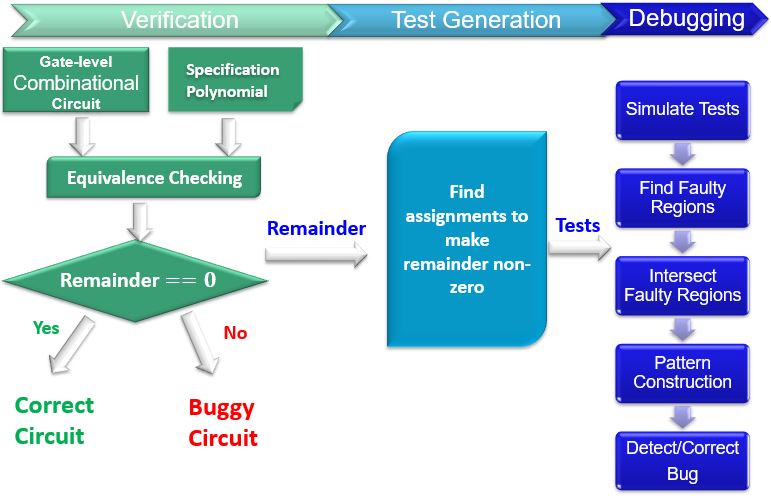
Existing equivalence checking techniques utilize Gröbner basis theory to produce a remainder to indicate the presence of a potential bug. However, bug localization remains a major bottleneck. Simulation-based validation using random or constrained-random tests are not effective and can be infeasible for complex arithmetic circuits. In our past projects, we developed an automated test generation and bug localization technique for debugging arithmetic circuits. Our approach is able to automatically generate directed tests by suitable assignments of input variables to make the reminder non-zero. The generated tests are guaranteed to activate the unknown bugs. We also proposed a bug detection and correction technique by utilizing the patterns of remainder terms as well as the intersection of regions activated by the generated tests. In her recent work, we have addressed the scalability concerns associated with equivalence checking that leads to an explosion in size of the remainder when the design is faulty. We developed an incremental equivalence checking method which is capable of localizing and correcting hard-to-detect bugs irrespective of their location in the design. In our current project, we plan to use Grobner basis theory for approximate hardware generation and its automatic debugging.
Related Publication:
- Automated test generation for debugging multiple bugs in arithmetic circuits
- Automated Debugging of Arithmetic Circuits Using Incremental Gröbner Basis Reduction
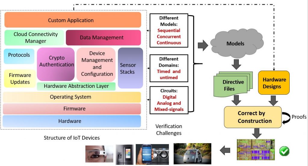
Design Automation of Modeling IoT Devices
Design of IoT devices starts with a high-level model of Internet-of-Things (IoT) devices as well as their constraints. Modeling of heterogeneous IoT devices, as well as their connectivity, is a major challenge due to the huge complexity coupled with the diversity of the computing models. After models and constraints are finalized, they should be validated and converted to actual hardware using efficient design exploration, fast prototyping, and effective design transformations. This modeling and validation would lead to the development of novel Electronic Design Automation (EDA) tools to enable automated generation of executable models and prototypes for CMOS as well as post-CMOS technologies. My research aims for correct-by-construction design automation methodology. In this project, we design EDA tools that generate high-level models based on the design constraints and perform verification of transformation steps from models to hardware chips. The automated framework would enable design exploration, automatic software generation, high-level synthesis, quick prototyping, and automatic patching. It is also extremely important to have EDA tools that can check for all vulnerabilities in all phases of the design since it may be infeasible to patch later. The tools must be able to predict various vulnerabilities such as reverse engineering, and fault injection attacks with warnings and possible solutions.
Related Publications:
- Security-aware FSM Design Flow for Identifying and Mitigating Vulnerabilities to Fault Attacks
- FSM Anomaly Detection Using Formal Analysis
Verification of IoT System-on-Chips
Modern SoC design technology has been a centerpiece in computing system architecture because of diverse applications such as smartphones, tablets, automotive systems, medical instruments, etc. It is very important to design robust and trustworthy SoCs. In this project, we plan to explore the following avenues to verify IoT SoCs, 1) use of analytics, formal validation, as well as machine learning techniques for scalable validation, and 2) streamlined architecture for effective post-silicon and in-field control and requirements update. Faster bug localization is one of the most important steps in design validation. A major problem with design validation is that we do not know whether a bug exists, and how to quickly detect and fix it. In this project, we use machine learning to implement verification tools that automatically detect the source of errors based on prior knowledge and verification efforts. The goal of this research is to reduce validation efforts by avoiding debugging known failures. In this project, we also plan to generate test patterns using machine learning. While directed tests can check for known errors, machine learning can extend to scope for both known and unknown (e.g., known errors with minor or major variations) SoC functional vulnerabilities.
We also aim for effective utilization of three widely used formal methods (equivalence checking, model checking, and theorem proving) for scalable validation techniques. Effective in-field debug should be performed in the case of buggy fabricated silicon. Post-silicon validation and debug is critical for IoT applications, where the device may need to be updated during its long lifetime, or in response to changing functional needs or new requirements.
Current Sponsor: Cisco
Related Publication:
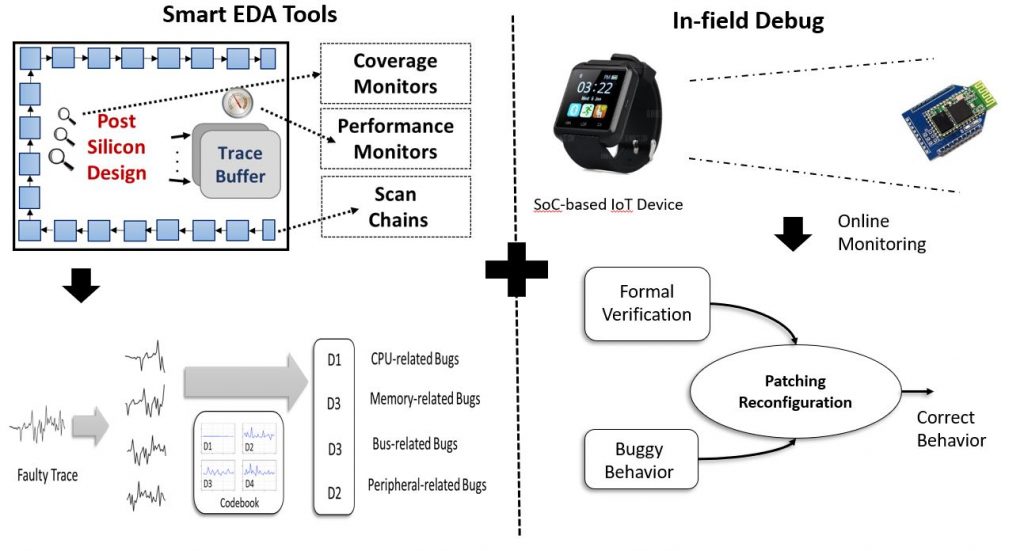
Post-Silicon Validation and Debug
Post-silicon validation is widely acknowledged as a major
In our past project, we proposed novel post-silicon validation techniques to ensure the correct behavior of silicon designs based on coverage analysis. Currently, there is no effective way to collect coverage of certain properties and events directly and independently on silicon. We explored how to utilize on-chip
There is an inherent conflict between increasing the observability and trust. Although designing effective debug infrastructures can drastically reduce the post-silicon validation and debug efforts by increasing the observability, the extra observability can facilitate integrity issues such as trace buffer attack and scan-based side channel attack. We plan to explore designing debug infrastructures that they do not violate any integrity constraints.
Related Publications: